Our company is laser technologies and service provider. MB Laser fabrication technologies team of engineers and researchers develops laser-based technologies for moulded interconnect devices and laser surface modification for various application. Company has 5 technology IPR (based on know-how). Company manufactures high-additive-value products (using laser-induced selective metal deposition on dielectrics technology) in small scale, such as antennas, chip pads for electronic components, in-mould circuits and etc. MB Laser Fabrication Technologies provides high-tech laser microfabrication solutions and service. During years of implementing various industrial and scientific projects our team has gained beneficial expertise and know-how knowledge in the laser material processing field. Our main field of expertise includes circuit formation on various dielectric materials, metal surface modification for high lubrication, glass laser polishing.
Selective Surface
Activation Induced by Laser
CO2 laser glass
polishing
Metal surface
texturing
Technology for selective metal deposition on free shaped dielectric materials
Electric circuit traces formation on 3D shaped dielectrics is one of the highest challenges in 3D Mechatronic Integrated Devices (3D-MID). The Selective Surface Activation Induced by a Laser (SSAIL) method is an advanced technology for solving emerged production issues for electric traces. SSAIL contains 3 main steps: laser modification of the dielectric surface, chemical activation of modified areas and electroless plating of activated parts.
The 3D-MID (Mechatronic Interconnect devices) is a modern solution for today and future devices. MID is an integration of mechanical and electrical functions in injection molded (in case of plastics) or milled three-dimensional bodies. A part with electronic circuits directly integrated into a dielectric component – it offers material, weight and cost savings, by the elimination of connectors between separate PCBs, shortening process chain and integration of contact surfaces, e.g. for switches, sensors and antennas. 3D-MID has a great potential in automotive, aviation, lighting, computing or even medicine sectors where emerging innovation demands to increase the number of the electronic component into a device.
Technology offers laser writing speeds of up to 5m/s with galvanometric scanners, and herewith spatial plating pitch is kept narrow at 25µm for polymer. Spatial plating pitch for glasses, ceramics and transparent polymer can be achieved down to 3 µm. The main advantages of the SSAIL process comparing with the alternative methods, is that SSAIL can form electric circuit on standard dielectric materials and does not require special additives inside bulk, unlike LDS (Laser direct structuring) does not use metalorganic additives. Therefore, SSAIL could open a broad area of application where current methods of electronics integration are still too expensive.

Another advantage is related with SSAIL capability to process transparent and flexible polymers, ceramics, glasses or even silicon.
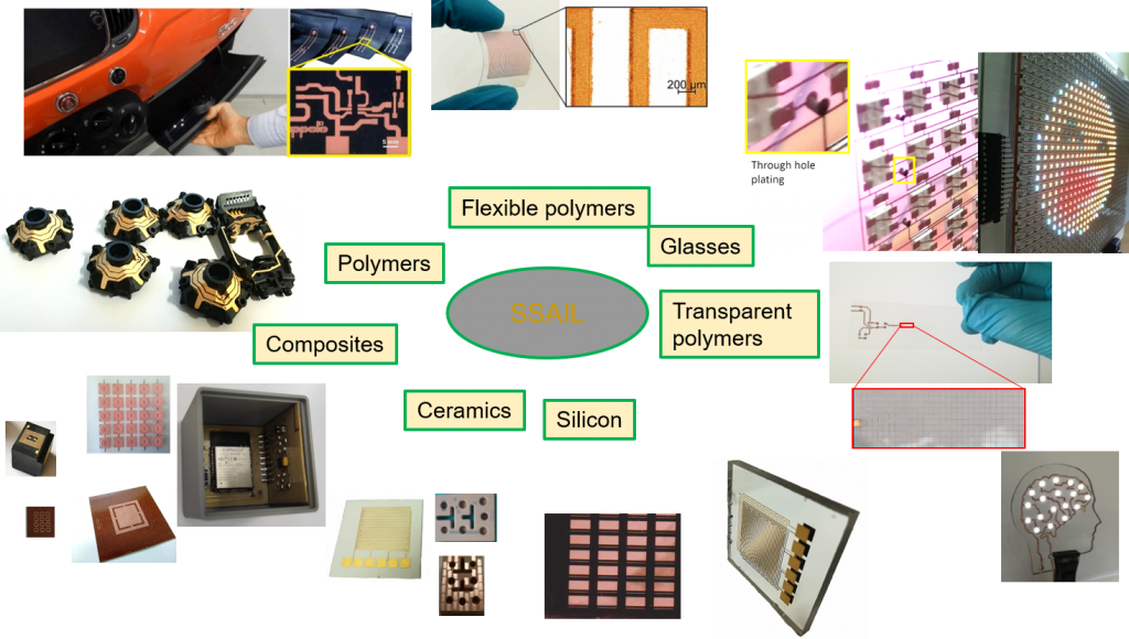
Polymers – polycarbonate (PC), acrylonitrile butadiene styrene (ABS), polycarbonate acrylonitrile butadiene styrene blend (PC/ABS), polyamide (PA), Polyamide 4 (PA4) poly vinyl chloride (PVC), polyphthalamide (PPA), Poly-methyl methacrylate (PMMA), Polyether ether ketone (PEEK), liquid crystal polymer (LCP), ABS for 3D printing, Polyethylene Terephthalate (PET), Polybutylene terephthalate (PBT), polyimide (PI), Polyphenylene Sulfide (PPS), Phenol formaldehyde resin (PF), epoxy, cyanate esters (ABF), Epoxy resin, Polybutylene succinate (PBS), Polytetrafluoroethylene (PTFE) known as Teflon.
Glass – soda lime, float glass, Fused silica.
Ceramics – SITAL ceramic, Al2O3 ceramic, AlNi.
Silicon (crystalline, microcrystalline, amorphous)
Composites (textolites) – Fr4, Getinax, RO3003™ Laminates (Rodgers), PREP 200 (preperm)
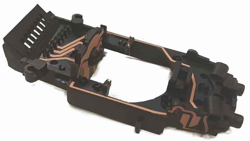
3D MID parts for automotive applications

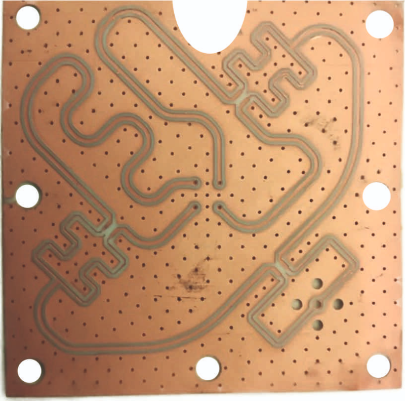
UHF fractal Antenna

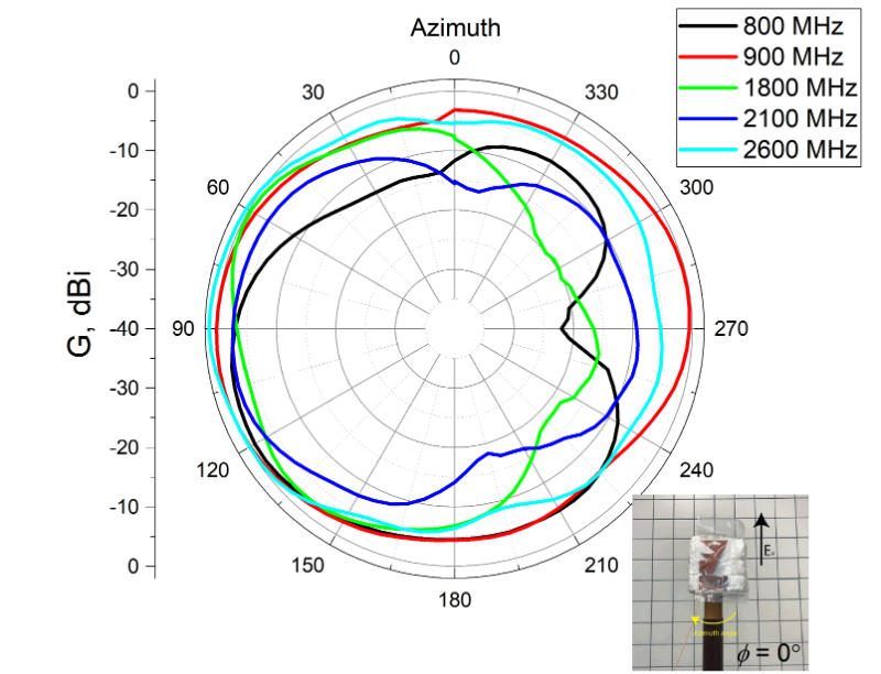
Conical antenna on 3D shaped PEEK plastic

Antenna on PTFE substrate
Meta-surface superstrate for resonance antenna, fabricated on flexible PET

LED matrix assembled on glass substrate with 2-layer circuit produced using

Electronic board assembled on fused silica. Produced using SSAIL


Every touchscreen is a device of numerous layers including a transparent conductive electrode. The current transparent conductive film market is dominated by expensive and fragile Indium-tin oxide electrodes, also known as ITO. However, ITO made from rare metal Indium. It results in a high-cost and brittle technology. There is a huge demand for alternative technologies to the ITO transparent electrode. New materials like carbon nanotubes, silver nanowires are still on the research stage and expensive as well. Most promising alternative is metallic mesh with metal wires less than 5 micrometers in diameter to be invisible but still electro-conductive. Our innovation allows us to produce a transparent – metal mesh electrode by electroless copper micro-plating technology induced by a precision laser writing.
Invisible metal mesh on glass and flexible PET for touch screen technologies. Produced using SSAIL.

Microelectrodes for cell’s temperature detections (Integrated in microscope slide)

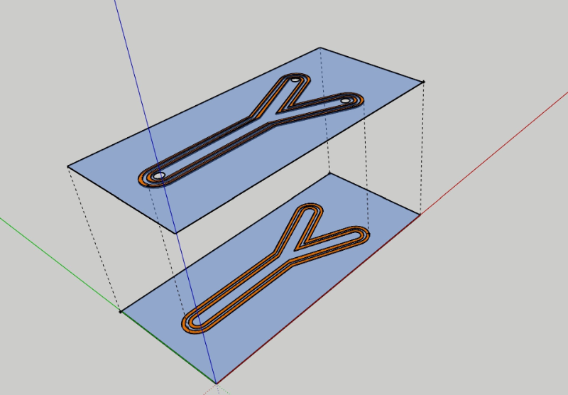
Channels for microfluidics applications
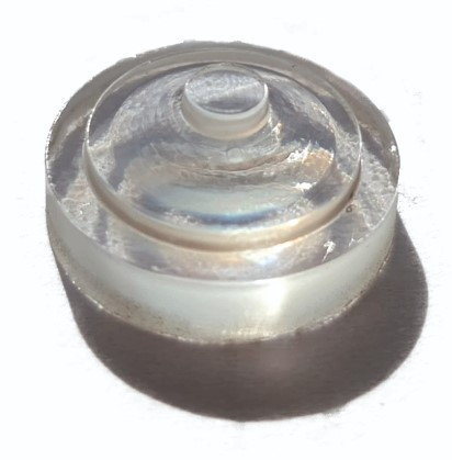
Glass is cheap and freely available, with attractive properties such as: resistance to temperature changes, chemicals, transparency in the visible and near IR zones. For these reasons, glass is the most commonly used material in the manufacture of optical elements.
In laser polishing, due to the amount of laser energy, two different regimes can be distinguished according to the difference between the melted layer thickness and the peak-valley distance. One is shallow surface melting (SSM) and the other is surface over melting (SOM). In SSM, the laser energy is not very large and the melted layer thickness is less than the peak-valley distance; thus, the peaks of the sample surface can be melted and flow into the valleys. In SSM, the surface roughness can be reduced to a large extent. In SOM, the large laser energy is irradiated onto the metallic surface, and not only the cap but also the whole particle is melted, and a melt pool is created. The ripple shapes are formed on the metal surfaces as depicted in Fig. 1 a.
Our company has knowledge how to implement both regimes at once. Our surface polishing technology allows to achieve surface roughness below 200 nm, using fast laser writing 1000 mm/s.

Before polishing

After polishing

Laser induced periodic surface structures have found many applications during the last decade: control of surface wetting; friction reduction; colouring the surfaces; light absorption enhancement. We provide laser patterning with controllable period varying from 200 nm to 600 nm of various materials (metals, polymers, glass)
Laser Induced Periodic Surface Structures for lubrication applications.

All rights reserved. © 2021
LASERFAB.LT